
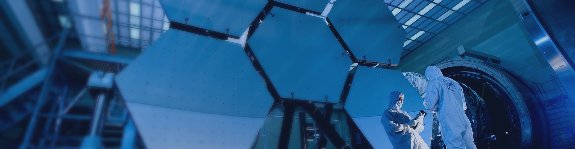
 en
en cn
cn

01
Crystal preparation technology
Crystals are mainly prepared using Vertical Gradient Freeze (VGF) technology.
Advantages of VGF:
- Simple technological process and good repeatability.
- Easy to implement program control.
- Shape determined by the crucible contour with high crystal utilization rate.
- Small temperature gradient, small crystal thermal stress, less defects, good crystalline perfection, etc.
02
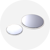
Substrate manufacturing technology
A technology for processing a crystal into a substrate, which can be used to manufacture semiconductor devices through several technological processes such as dicing, edging, grinding, polishing, cleaning, etc.
dicing
Multi-wire cutting technology is adopted, which is currently the most advanced cutting technology in the world. The high-speed steel wire drives the cutting edge material attached to the steel wire, to move backwards and forwards against a crystal bar, thus achieving the cutting effect.It has many advantages
Technical advantages of dicing
- small BOW and WARP
- good TAPER
- small total thickness tolerance (TTA) discreteness
- small cutting loss of cutting edge
- shallow surface damage layer
- small surface roughness of substrate, etc
03
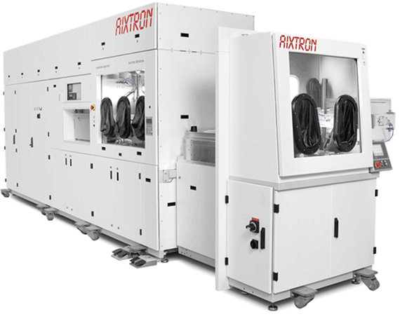
Epitaxial growth technology
MOCVD system imported from Germany is used. The epitaxial wafers are produced using internationally leading epitaxial growth technology.
The AIX 2800G4 system imported from Germany is an advanced thin film manufacturing system with a high utilization rate for growing epitaxial thin films for GaAs devices. With our special design of the epitaxial layer and precise control of various growing conditions, epitaxial wafers grown using this system have advantages of high consistency, good uniformity, good appearance and high comprehensive yield of various indexes, and they can fully meet customer requirements for various epitaxial wafer indexes.
04
Chip processing technology
Our company adopts leading domestic and foreign processing technologies to process epitaxial wafers by using evaporation, lithography, etching, cleaning, grinding and dicing, to produce chip products with corresponding functional applications.
-
01
evaporation
-
02
lithography
-
03
etching
-
04
cleaning
-
05
grinding
-
06
dicing

Lithography procedure
At present, we have the Canon I5 series lithography machine. The exposure line width accuracy can be greatly reduced using our unique multi-exposure technology, and the minimum line width can reach about half of the line width when using standard lithography machines.
Etching procedure
We possess a variety of etching monitoring technologies for accurate etching monitoring of the etching target film layer. Our technology features high etching accuracy, strong controllability and high yield.

Grinding procedure
We use the automatic grinder to reduce the thickness of chip wafers. The thickness of the wafer is generally about 650μm, and the final chip thickness is usually less than 100μm.
Dicing procedure
Our cutting process features characteristics of high cutting efficiency, high precision and high yield, and can fully meet the requirements of different customers for wafer materials.
Fully automatic AOI sorting procedure
We have several imported fully automatic AOI inspection equipment. AOI (Automatic Optical Inspection) allows 2D/3D optical visual inspection with inspection accuracy up to the micron level, for linked grade classification using the automatic die sorter, which fully guarantees the controllability of shipped chips’ appearance yield.
 粤公网安备 44180302000129号