
 en
en cn
cn

Gallium Arsenide Substrates
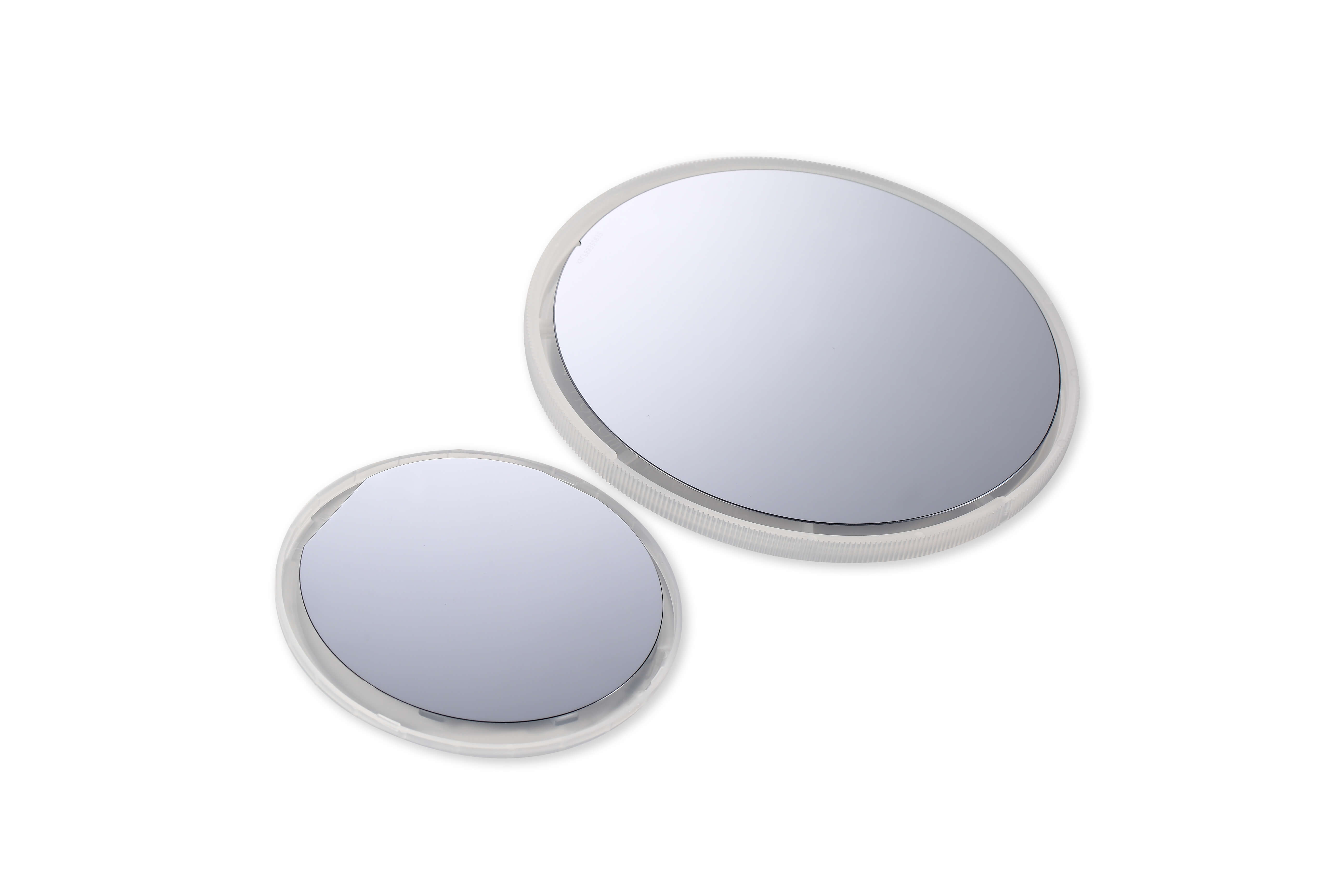
We provide GaAs substrates with a maximum size of 6 inches, grown using VGF technology, including semi-insulating GaAs wafers (un-doped) and semi-conducting GaAs wafers (Si or Zn doped).
Gallium Arsenide (GaAs) is an excellent semiconductor material with direct band gap, high electron mobility, high-frequency and low noise, and high conversion efficiency. Gallium Arsenide is widely used in optoelectronic and microelectronic industries.

Gallium Arsenide (GaAs) is an excellent semiconductor material with direct band gap, high electron mobility, high-frequency and low noise, and high conversion efficiency. Gallium Arsenide is widely used in optoelectronic and microelectronic industries.
| Item | Unit | LD Applications Specifications | LED Applications Specifications | Microelectronics Specifications |
|---|---|---|---|---|
| Conduction Type | N-type | P-type/N-type | ||
| Crystal Growth Method | VGF | VGF | VGF | |
| Dopant | Si | Zn/Si | Undoped | |
| Diameter | inch | 2",3",4" and 6" | 2",3",4" and 6" | 2",3",4" and 6" |
| Wafer Orientation* | (100)±0.1° | (100)±0.5° | (100)±0.5° | |
| OF/IF | US or EJ | US or EJ | US, EJ or notch | |
| Carrier Concentration | /cm3 | (0.4-2.5) ×1018 | (0.5-5) ×1019 (0.4-4)×1018 |
|
| Resistivity | ohm.cm | (1.2-9.9) ×10-3 | (1.2-9.9)×10-3 | >107 |
| Mobility | cm2/v.s | >1500 | 50-120/>1000 | >4000 |
| Etch Pit Density | /cm2 | <500 | <5000 | <5000 |
| Laser Marking | Upon request | Upon request | Upon request | |
| Thickness* | μm | (350-650)±25 | (350-650)±25 | (350-650)±25 |
| TTV(P/P) | μm | ≤5 | ≤5 | ≤4 |
| TTV(P/E) | μm | ≤10 | ≤10 | ≤10 |
| Warp | μm | ≤10 | ≤10 | ≤10 |
| Surface | Side 1 Side 2 |
Polished Polished/Etched |
Polished Polished/Etched |
Polished Polished/Etched |
| Epi-ready | Yes | Yes | Yes | |
| Package | Cassette or single wafer container | Cassette or single wafer container | Cassette or single wafer container |
 share it


 粤公网安备 44180302000129号