
 en
en cn
cn

Indium Phosphide (InP) Substrates
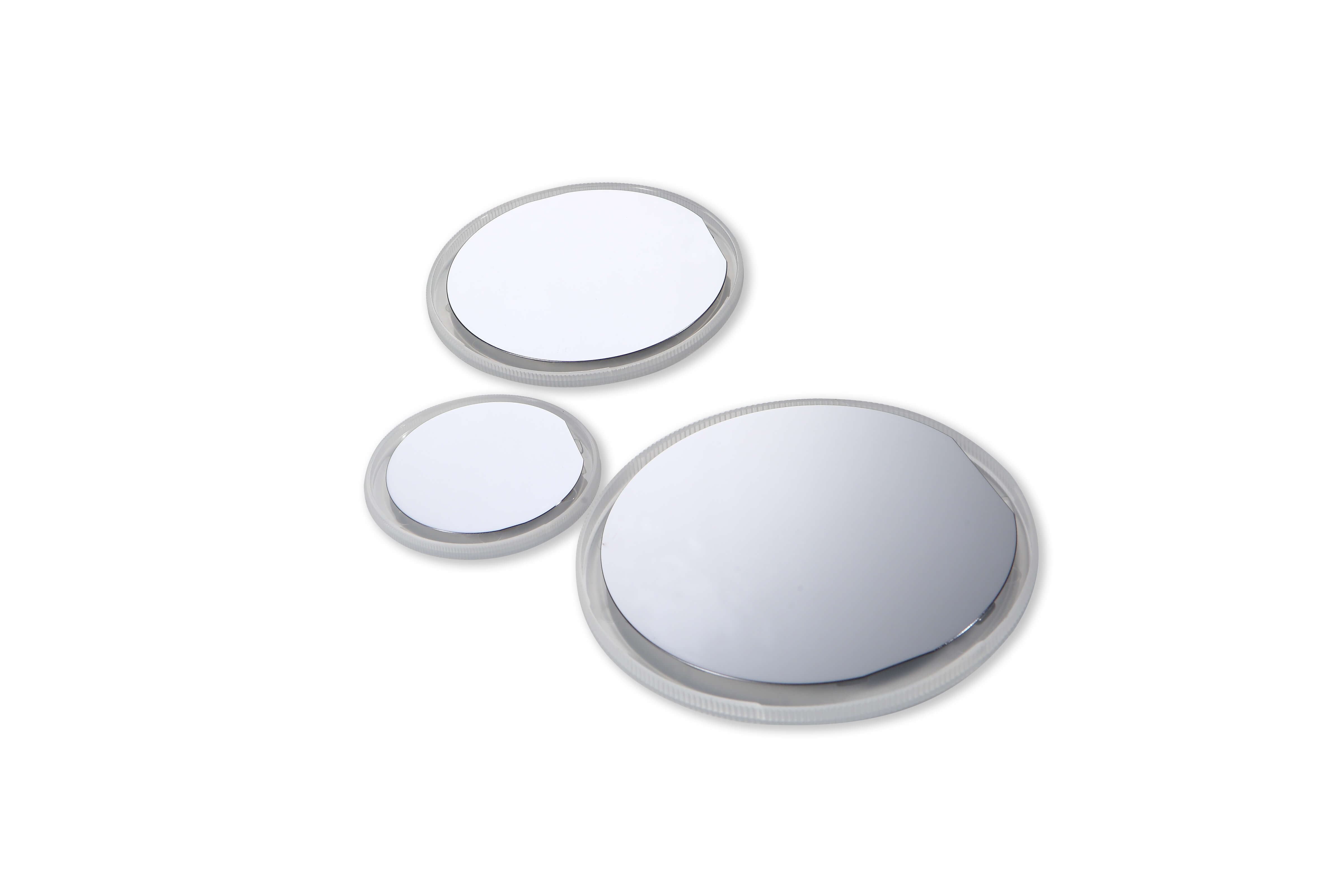
CS Microelectronics supplies high-quality Indium Phosphide (InP) wafers, with diameter ranging from 2”to 4”. InP wafer are provided un-doped, Fe-doped, S-doped , and Zn-doped.
InP is an important III-V compound and semiconductor material. It has advantages of high electron mobility, good radiation stability and large band gap. Indium Phosphide is widely used in optoelectronic and microelectronic industries.

InP is an important III-V compound and semiconductor material. It has advantages of high electron mobility, good radiation stability and large band gap. Indium Phosphide is widely used in optoelectronic and microelectronic industries.
| Item | Unit | Semi-insulating Specifications | Semiconductor Specifications |
|---|---|---|---|
| Conduction Type | N-type/P-type | ||
| Crystal Growth Method | VGF | VGF | |
| Dopant | Fe | S, Sn/Undoped/Zn | |
| Diameter | inch | 2",3",4" | 2",3",4" |
| Wafer Orientation* | (100)±0.5° | (100)±0.5° | |
| OF/IF | US,EJ | US,EJ | |
| Resistivity (Res) | ohm.cm | ≥0.5x10⁷ | |
| Carrier Concentration (C.C) | cm-3 | N/A | (0.8-8)x1018/(1-10)x1015/(0.8-8)x1018 |
| Mobility (Mob) | cm2/v.s | ≥1000 | 1000-2500/3000-5000/50-100 |
| Etch Pit Density (EPD) | /cm2 | 1500-5000 | 100-5000/≥5000/≥500 |
| Laser Marking | Upon request | Upon request | |
| Thickness* | μm | (350-675)±25 | (350-675)±25 |
| TTV(P/P) | μm | ≤10 | ≤10 |
| TTV(P/E) | μm | ≤15 | ≤15 |
| Warp | μm | ≤15 | ≤15 |
| Surface | Sides 1 & 2 | Polished/Etched | Polished/Etched |
| Epi-ready | Yes | Yes | |
| Package | Cassette or single wafer container | Cassette or single wafer container |
 share it


 粤公网安备 44180302000129号